
Download the pdf to keep learning offline. Clock signals, analog signals, rf signals, etc.
PCB Component Placement Guidelines Tips & Tricks

Resistance is a physical property of the metal used to make the trace.
Pcb design tips and tricks pdf. Up to 10% cash back it is one of the most used software for electronic design. Route these traces first, with the most desirable layout. Pcb designers most commonly use length, thickness, and width to control the resistance of a pcb trace.
Traces 12.5 resistance of conductors 12.5 voltage drop in signal leads—kelvin feedback 12.7 signal return currents 12.7 ground noise and ground loops 12.9 ground isolation techniques 12.11 static pcb effects 12.15 Printed circuit board (pcb) design issues introduction 12.1 section 12.1: Now you can choose your aim to save the data in other formats.
There is a bunch of tips and tricks in altium. In this issue, we have you covered. • identify the most critical traces in the design:
Introduction to high speed pcb designing: •build bill of materials with components supplier. Pcb trace thickness is measured in ounces of copper.
Simply click the x key every time you want to add a vertex during routing. "new objective, get from point a. 100 game design tips and tricks pdf free download without clear goals, players won't know what to do in your game and as a result, won't feel engaged.
This ebook will discuss multiple ways good pcb design can help manage emi interference on your board. Goals communicated to the player by the game itself for example: For some good insider information on pcb design, check out these pcb layout tips here.
Place the test points at the edge of the board to avoid wires hanging over the circuit on which you're trying to work. The free, open source software allows you to create pcb layouts and schematics. Eurocircuits' pcb tips & tricks cover all design related issues and their influence on manufacturing.
This document provides tips and tricks for using allegro pcb editor. Wire loop hook test points. It also covers usage and examples to customize the environment to maximize productivity.
Click the pdf above to read more about high speed design in this presentation. It is an amazing experience to hold in your hand the manufactured printed circuit board that resulted from the schematic that you captured. The goal of schematic capture:
Looped wire test points pcb layout. Audience this document is intended for allegro pcb editor users who wish to maximize the performance of allegro pcb editor for their environment. It covers tips and tricks like using emi cans for shielding, proper grounding techniques, trace length, isolating ac and dc signals and differential pair routing.
This command is only available in the placement edit and in orcad pcb designer professional or allegro pcb designer. For the loop itself, i tend to use wire cut off from component leads. Pcb designers can't really change the physical properties of copper, so focus on the trace size, which you can control.
Eagle cad tips and tricks may 09, 2016 by yahya tawil most hobbyists and many professionals use eagle cad as a daily tool in designing schematics and laying out pcb. •most important step in designing a pcb. Click the pdf above to read more about pcb design techniques to reduce emi in this ebook.
The time you spent preparing for this career and studying. Learning altium is useful for everyone planning or already working in electronics. • maintain at least a 3x trace width separation around constantly switching traces like clocks (avoids crosstalk) • you are smarter than the auto router software, so don't use it.
The menus and dialog boxes are engineered to be intuitive, and easy for new users to navigate through. A better solution is to add a couple of test points when you design the circuit board. •be aware of package size/code.
Pcb editor tips and tricks © 2021 parallel systems limited page 17 of 42 • save steps: High speed tips and tricks. Tips and tricks «design reuse» a simple way to reuse a part of an existing design is to use the place replicate command.
In this unite 2016 talk, curtiss vlurphy talks about 3 kinds of goals:

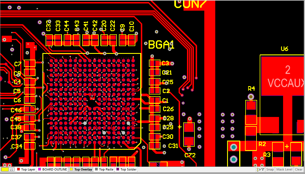
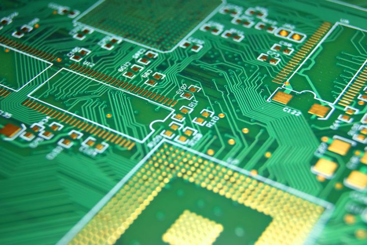
Pcb Design Tips And Tricks Pdf PCB Designs
Easier PCB Design EAGLE CAD Tips and Tricks

TIPS & TRICKS for PCB Designing& Assembly PCB Assembly
Pcb Design Tips And Tricks Pdf PCB Designs


How to make a PCB at home easily Part 1 PCB designing
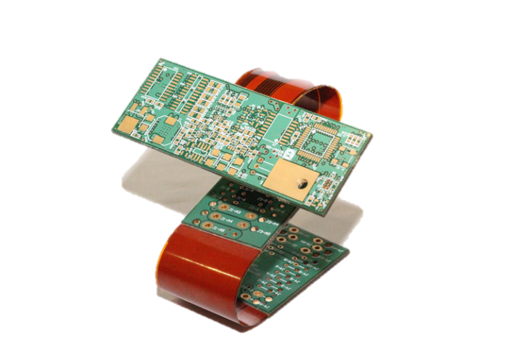
FLEXIBLE PCB DESIGN TIPS AND TRICKS PreventLAB
TIPS & TRICKS for PCB Designing& Assembly PCB Assembly
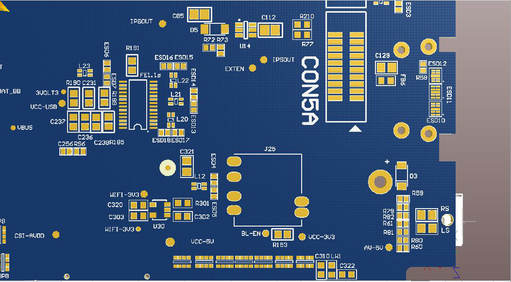
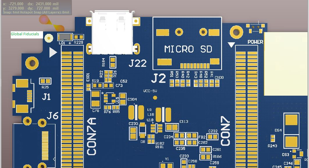
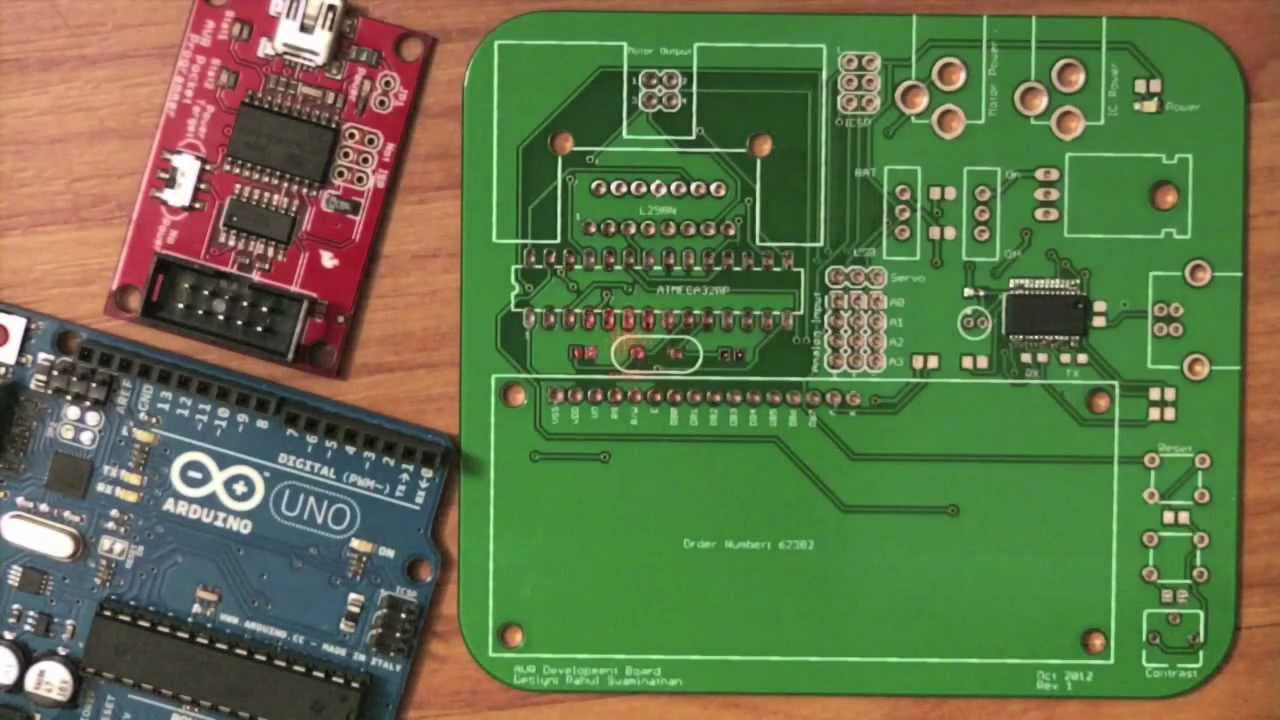
PCB Layout.pdf

Solving Modern PCB Layout Challenges Altium
Best PCB Design Tips Altium
Hardware Hacking PCB Layout and Etching Tips and Tricks


High Power PCB Design Tips & Tricks MicroType Engineering
TIPS & TRICKS for PCB Designing& Assembly PCB Assembly
Top 5 PCB Design Tricks And Tips For Complete Beginners
Time Saving Tips and Tricks in Altium Designer Part 2 PCB
Tips and Tricks for an Efficient PCB Layout Blog PCB

Design Tips for Positioning an Embedded Antenna on a PCB
PCB Design Tips General Electronics Tutorial YouTube

Pcb Design Tips And Tricks Pdf PCB Designs